Pages

Showing posts with label electronics. Show all posts

Thursday, 24 February 2011

what is transistor

transistor is a semiconductor device used to amplify and switch electronic signals. It is made of a solid piece of semiconductor material, with at least three terminals for connection to an external circuit. A voltage or current applied to one pair of the transistor's terminals changes the current flowing through another pair of terminals. Because the controlled (output) power can be much more than the controlling (input) power, the transistor provides amplification of a signal. Today, some transistors are packaged individually, but many more are found embedded in integrated circuits

Transistor as a switch

BJT used as an electronic switch, in grounded-emitter configuration.
Transistors are commonly used as electronic switches for both high- and low-power applications such as switched-mode power supplies and logic gatesrespectively.
In a grounded-emitter transistor circuit, such as the light-switch circuit shown, as the base voltage rises the base and collector current rise exponentially, and the collector voltage drops because of the collector load resistor. The relevant equations:
VRC = ICE × RC, the voltage across the load (the lamp with resistance RC)
VRC + VCE = VCC, the supply voltage shown as 6V
If VCE could fall to 0 (perfect closed switch) then Ic could go no higher than VCC / RC, even with higher base voltage and current. The transistor is then said to be saturated. Hence, values of input voltage can be chosen such that the output is either completely off,[13] or completely on. The transistor is acting as a switch, and this type of operation is common in digital circuits where only "on" and "off" values are relevant.

[edit]Transistor as an amplifier

Amplifier circuit, common-emitter configuration.
The common-emitter amplifier is designed so that a small change in voltage in (Vin) changes the small current through the base of the transistor and the transistor's current amplification combined with the properties of the circuit mean that small swings in Vin produce large changes in Vout.
Various configurations of single transistor amplifier are possible, with some providing current gain, some voltage gain, and some both.
From mobile phones to televisions, vast numbers of products include amplifiers for sound reproductionradio transmission, and signal processing. The first discrete transistor audio amplifiers barely supplied a few hundred milliwatts, but power and audio fidelity gradually increased as better transistors became available and amplifier architecture evolved.
Modern transistor audio amplifiers of up to a few hundred watts are common and relatively inexpensive.

[edit]

Advantages

The key advantages that have allowed transistors to replace their vacuum tube predecessors in most applications are
  • Small size and minimal weight, allowing the development of miniaturized electronic devices.
  • Highly automated manufacturing processes, resulting in low per-unit cost.
  • Lower possible operating voltages, making transistors suitable for small, battery-powered applications.
  • No warm-up period for cathode heaters required after power application.
  • Lower power dissipation and generally greater energy efficiency.
  • Higher reliability and greater physical ruggedness.
  • Extremely long life. Some transistorized devices have been in service for more than 50 years.
  • Complementary devices available, facilitating the design of complementary-symmetry circuits, something not possible with vacuum tubes.
  • Insensitivity to mechanical shock and vibration, thus avoiding the problem of microphonics in audio applications.

How to make a Rheostat


Although the below explained process is not applicable for any electronic circuits, you will clearly get a clear idea on how a rheostat works.

Components

  1. The components needed for the connection are
  2. Flashlight bulb and socket [1]
  3. Dry cell lantern battery/D-cell battery [2]
  4. Wire [About 15 to 17 inches and another one 2 inches]
  5. Spring [1]
  6. Wire Clippers [A pair]
  7. A typical spring can be obtained from a widow roll up. You can even get to buy one at a cheap rate.

Procedure

  • Connect the two Dry cell lantern/D-cell batteries tail-to-tail, so that the positive polarity of one battery is connected to the negative polarity of the other.
  • Using a wire cutter, cut the wire in equal lengths. One wire should be at least 8 centimetres long.
  • Connect the wires onto the open ends of both the batteries.
  • The end of one wire must be connected to the bulb socket with the bulb in it.
  • Connect the second wire to one end of the long spring.
  • Connect the free end of one wire to one terminal of the light socket.
  • Connect the other free wire to one end of the spring.
  • Take the two inch wire and connect it to the second terminal of bulb socket.
  • Connect the other end of the two inch wire onto the other end of the spring.
How to make a RheostatHow to make a Rheostat

How to make a Rheostat

What happens?

As soon as the circuit is in closed loop, the bulb begins to glow. Although the glow intensity is less, when you move the wire through the spring onto the other end where the wire is connected, the bulb starts to glow more brightly. When both the wires are nearby the glow will be in its maximum.
The spring is mainly made of steel wire. Steel wires are not very good conductors of electricity. Thus the resistance of the circuit also increases. If the spring length is long enough you will get to see different stages of the glow. Thus you will get to see the working of a rheostat.

MOSFET Technology and Various MOS Process


MOSFET Technology and Various MOS Process

This article focuses on basics of MOSFET Technology,basics of various MOS process like p-channel MOS (PMOS), n-channel MOS (NMOS), Complimentary MOS (CMOS) – its manufacturing, cross section, and other advantages of one over other.
Most of the LSI/VLSI digital memory and microprocessor circuits is based on the MOS Technology. More transistor and circuit functions can be achieved on a single chip with MOS technology, which is the considerable advantage of the same over bipolar circuits. Below given are the reasons for this advantage of MOS technology:
  • Less chip area is demanded by an Individual MOS transistor, which results in more functions in less area.
  • Critical defects per unit chip area is low for a MOS transistor because it involves fewer steps in the fabrication of a MOS transistor.
  • Dynamic circuit techniques  are practical in MOS technology, but not in bipolar technology. A dynamic circuit technique involves use of fewer transistors to realise a circuit function.
So you are already clear that because of above said reasons, its considerably cheap to use MOS technology over Bipolar one.
Three types of MOS process are PMOS, NMOS and Complimentary MOS. Let’s take a look at brief descriptions below.

p-Channel MOS or PMOS Technology

This MOS process operates at a very low data rate say 200Kbps to 1Mbps. PMOS is also considered as the first MOS process which required special supply voltages as -9 volts, -12 volts and so on.

n-Channel MOS  or NMOS Technology

We can say this is a second generation MOS process, after PMOS, which has considerable improvement in data rates; say up to 2Mbps and resulted in the construction of LSI circuits of a single standard +5volt supply.NMOS increases circuits speed in sharp, because of reduction in the internal dimensions of devices; which is contrary to (and an advantage over) bipolar circuits whose speed increases gradually.The difference in performance between both circuits have steadily become smaller for both LSI and VLSI because of steady improvements in pattern definition capability.
Have you ever heard of Self aligned silicon gate NMOS ? It’s a commonly used and popular version of MOS technology. Now a days, a technique named as local oxidation is used for this process to improve circuit density and performance. HMOS, SMOS and XMOS are the commonly used names by manufacturers for this. Older versions of the process like Metal Gate NMOS and PMOS are not used now a days for latest designs. A second layer of poly-silicon may be added to the process for important memory applications.

Complementary MOS Technology

So you might have already got an idea from the name “Complimentary MOS” ? Its a combination of both n-channel and p-channel devices in one chip. Compared to both other process, CMOS is complex in fabrication and requires larger chip area. Biggest advantage of a CMOS circuit is reduced power consumption (less than NMOS); it is designed for zero power consumption in steady state condition for both logic states. As you may already know, CMOS circuits are widely used in digital equipments like watches, computers etc.
CMOS offers comparatively higher circuit density and high speed performance (used in VLSI);and this is the primary reason why CMOS is still preferred despite it’s complex manufacturing process. Memories and microprocessors made of CMOS usually employ silicon gate process.
There are variations of MOS technology which offer either better performance or density advantages over the standard process. Some of those are named as VMOS (V-groove MOS), DSA (Diffusion Self Aligned), SOS (Silicon on Saphire), D-MOS (Double diffused MOS) etc.

Simple MOSFET Structures

MOS Technology comprises of 3 process basically, p-channel MOS, n-channel MOS and CMOS process. The basic purpose of all these process is to enhance MOSFET performance one over the other, like lower power consumption, high power capability, relaibility improvements, response speed etc.

PMOS Structure

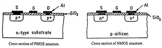
The PMOS is the first device made in metal gate p-channel technology. PMOS infact is an older version of the MOS process which is not used nowadays. A cross sectional view of the PMOS structure is shown below.

PMOS and NMOS Structures
The starting material is a single crystal Si that is doped n-type with phosphorus or antimony with a doping level on the order of 1015 atoms/cm3.
So the process is like this, first grow a relatively thick oxide layer; say 1.5micros and then etch windows for the source to drain diffusion. As a next step we have to boron dope the source and drain regions with 2 to 4 micro meters depth. Lets next form the gate oxide, that serves as the dielectric used for turning ON and OFF the MPS device. The entire circuit is then metalised and etched so that there is metal over the gate, drain, and the source. The metal layer should be 1 to 2 micrometers thick and is deposited using an electron beam evaporator.

NMOS Structure:

An NMOS structure also follows a similar pattern or sequence as shown in the crosssectional figure above; and is similar to PMOS except for the n+ regions which are diffused into the p-type silicon substrate.

Wednesday, 23 February 2011

Automatic night light circuit


Automatic night light circuit

Description.
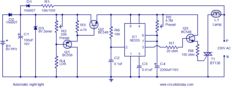
A cheap and simple automatic night light using few transistors and NE555 timer is shown here. The circuit will automatically switch on the AC lamp when night falls and the lamp will be automatically switched off after a preset time.
The working of this night light circuit very simple. An LDR is used as the sensor here. At day time the resistance of the LDR will be low and so do the voltage drop across it, the transistor Q1 will be in the conducting mode. When darkness falls the resistance of LDR increases and so do the voltage across it. This makes the transistor Q1 OFF. Base of Q2 is connected to the emitter of Q1 and so Q2 is biased on which in turn powers the IC1. NE555 is wired as monostable multivibrator that is automatically triggered at power ON. This automatic triggering is achieved with the help of capacitor C2. The output of IC1 remains high for a time determined by resistor R5 and capacitor C4. When output of IC1 goes high transistor Q3 is switched ON which triggers triac T1 and the lamp glows. A 9V battery is included in the circuit in order to power the timer circuit during power failures. Resistor R1, diode D1, capacitor C1 and Zener D3 forms the power supply section of the circuit. R7 and R8 are current limiting resistors.
Circuit diagram of automatic night light.
night light cicuit
Automatic night light circuit

fire alarm circuit


Description.
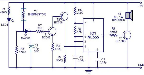
Many fire alarm circuits are presented here,but this time a new circuit using a thermistor and a timer to do the trick. The circuit is as simple and straight forward so that , it can be easily implemented.The thermistor offers a low resistance at high temperature and high resistance at low temperature. This phenomenon is employed here for sensing the fire.
The IC1 (NE555) is configured as a free running oscillator at audio frequency. The transistors T1 and T2 drive IC1. The output(pin 3) of IC1 is couples to base of transistor T3(SL100), which drives the speaker to generate alarm sound. The frequency of NE555 depends on the values of resistances R5 and R6 and capacitance C2.When thermistor becomes hot, it gives a low-resistance path for the positive voltage to the base of transistor T1 through diode D1 and resistance R2. Capacitor C1 charges up to the positive supply voltage and increases the the time for which the alarm is ON. The larger the value of C1, the larger the positive bias applied to the base of transistor T1 (BC548). As the collector of T1 is coupled to the base of transistor T2, the transistor T2 provides a positive voltage to pin 4 (reset) of IC1 (NE555). Resistor R4 is selected s0 that NE555 keeps inactive in the absence of the positive voltage. Diode D1 stops discharging of capacitor C1 when the thermistor is in connection with the positive supply voltage cools out and provides a high resistance path. It also inhibits the forward biasing of transistor T1.
Circuit diagram with Parts list.
fire-alarm-circuit.jpg

Static 0 to 9 display


Description.
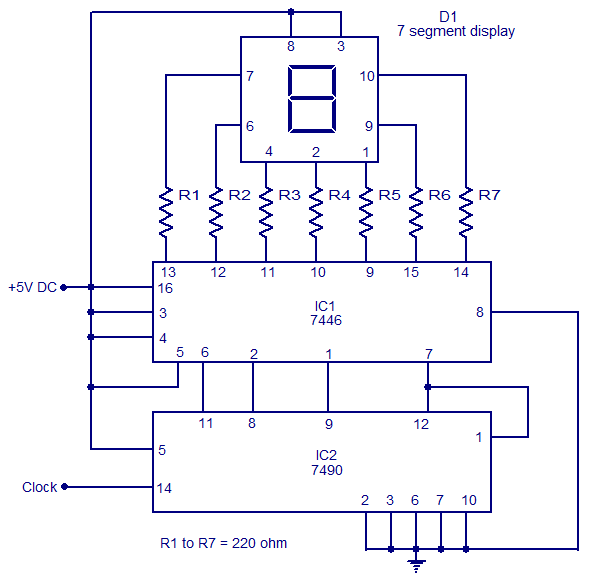
The circuit shown here is of a simple 0 to 9 display that can be employed in a lot of applications. The circuit is based on asynchronous decade counter 7490(IC2), a 7 segment display (D1), and a seven segment decoder/driver IC 7446 (IC1).
The seven segment display consists of 7 LEDs labelled ‘a’ through ‘g’. By forward biasing different LEDs, we can display the digits 0 through 9. Seven segment displays are of two types, common cathode and common anode. In common anode type anodes of all the seven LEDs are tied together, while in common cathode type all cathodes are tied together. The seven segment display used here is a common anode type .Resistor R1 to R7 are current limiting resistors. IC 7446 is a decoder/driver IC used to drive the seven segment display.
Working of this circuit is very simple. For every clock pulse the BCD output of the IC2 (7490) will advance by one bit. The IC1 (7446) will decode this BCD output to corresponding the seven segment form and will drive the display to indicate the corresponding digit.
Circuit diagram.
0 to 9 display


Frequency to voltage converter using LM331


Description.
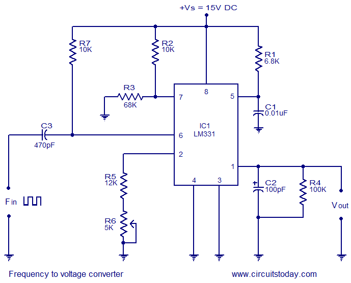
LM331 is basically a precision voltage to frequency converter from National Semiconductors. The IC has a hand full of applications like analog to digital conversion, long term integration, voltage to frequency conversion, frequency to voltage conversion. Wide dynamic range and excellent linearity makes the IC well suitable for the applications mentioned above.
Here the LM331 is wired as a frequency to voltage converter which converts the input frequency into a proportional voltage which is extremely linear to the input frequency. The frequency to voltage conversion is attained by differentiating the input frequency using capacitor C3 and resistor R7 and feeding the resultant pulse train to the pin6 (threshold) of the IC. The negative going edge of the resultant pulse train at pin6 makes the built-in comparator circuit to trigger the timer circuit. At any instant, the current flowing out of the current output pin (pin 6) will be proportional to the input frequency and value of the timing components (R1 and C1). As a result a voltage (Vout) proportional to the input frequency (Fin) will be available across the load resistor R4.
Circuit diagram.
frequency to voltage converter using LM331

Fan speed controller using LM2941


Description.
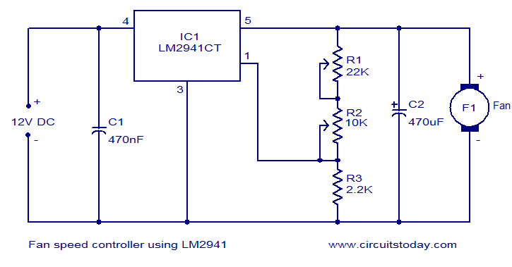
Many electronic circuits related to fan speed controlling have been published here and this one is just another approach. The circuit diagram shown here is of 12V DC fan speed controller using the IC LM2941CT which is a low drop out 1A voltage regulator. The IC has a dropout voltage as low as 0.5 and has also many useful features like power supply reverse protection, thermal protection, short circuit protection etc. The maximum output current the IC can source is 1A.
The 12V DC supply is connected between the Vin (pin4) and ground (pin3) of the IC. The load, which is the fan, is connected across the Vout (pin5) and ground (pin3) of the IC. The network comprising of potentiometers R1, R2 and resistor determines adjust current (Iadj) of the IC. By varying the Iadj using the POT R2 we can adjust the output voltage of the IC and hence the fan speed.
Circuit diagram.
fan speed controller using LM2941


Monday, 21 February 2011

Final Year Projects,Paper Presentations


                                         www.sourceforge.net     //contains around 3,60,000 completed project world biggest resource
                                        www.1000projects.com   //contains so many final year projects, paper presentation with good explanation,  and lab programs in mini project section.


Paper Presentations:   www.1000projects.com